
Chapter 4 of 8
Borrow a different byte at the same address
A 6809 pointer fits in two bytes. It can name 65,536 locations, yet a 512 KB CoCo 3 has eight times that much RAM. The GIME, the chip that manages memory and video in the CoCo 3, chooses which physical memory answers each CPU address. You can catch it answering the same question two different ways.
Translate one address by hand
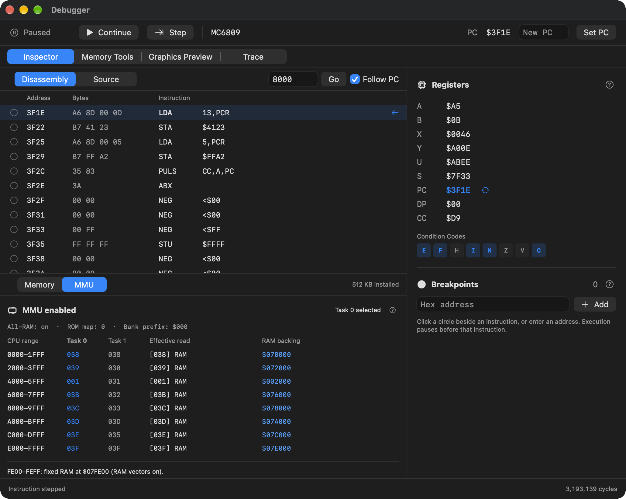
Open a fresh Disk BASIC setup with 512 KB. In Debug → Show Debugger, choose Inspector → MMU. The eight rows divide the CPU’s address space into windows of $2000 bytes (8 KB). Read the active task. Task 0 and task 1 are two sets of bank selections. CPU reads follow the active set when the MMU is enabled. RAM backing gives a physical RAM location. Effective read tells you whether the processor actually reads that RAM or a ROM overlay.
Find the row for CPU addresses $4000–$5FFF. On the practice machine the MMU is enabled, task 0 is active, and that row names bank $3A. The distance from $4000 to $4123 is $0123. Multiply the bank number by the bank size, then add the offset:
| Selection | Start of physical bank | CPU $4123 reads at |
|---|---|---|
| Bank $3A | $3A × $2000 = $74000 | $74123 |
| Bank $01 | $01 × $2000 = $02000 | $02123 |
In Memory, switch between Mapped CPU and Physical RAM. Look up $4123 in the first and $74123 in the second. Record the values. Equal bytes are consistent with the map; two zeros alone would be poor evidence that the addresses are connected. Give the second bank a distinctive byte and the connection becomes visible.
Borrow block 2
Save bankwalk.asm and open that copy in Assembly Development. Use the fresh setup above. Before running, check that block 2 has effective RAM reads, the initial bank is $3A and the code starts at $3F00. If the mapping differs, stay with read-only inspection until you have the practice configuration. This example deliberately changes a machine register. Finish its restoration before running anything else.
start       pshs    cc,a            ; preserve incoming flags and A
            orcc    #$50            ; hold IRQ and FIRQ until restored
            lda     bank2
            anda    #$3f            ; 512 KB supplies six bank bits
            sta     oldbank,pcr
            lda     #1
            sta     bank2           ; window now sees physical $02123
            lda     window
            sta     oldbyte,pcr     ; keep the byte even on a fresh machine
            lda     #$a5
            sta     window
inspect     lda     oldbyte,pcr     ; pause BEFORE this instruction
            sta     window          ; put the borrowed byte back
            lda     oldbank,pcr
            sta     bank2           ; restore the original translation
The program saves its incoming flags and masks IRQ and FIRQ. It saves the six bank bits the 512 KB machine implements. Then it writes $01 to $FFA2, the task 0 register for block 2. From that instruction onward, an ordinary read or write at $4123 goes to the borrowed bank. The program remembers the byte already there, writes $A5, and leaves an instruction labeled inspect for you. The code and saved bytes live in block 1. The running BASIC stack is in block 3. Neither is moved by that register write.
Catch the mapping in the act
- Choose Debug from Entry. Read the addresses of inspect and restored in Build details. In the supplied build they are $3F1E and $3F2C.
- Open the machine Debugger. Add those two hexadecimal addresses in Breakpoints, then use the debugger’s Continue. These are CPU address stops; assembly source debugging checks the memory mapping attached to its build. The address stops let you observe a deliberate mapping change.
- At inspect, read the MMU row again. Task 0, block 2 now selects $01. In Mapped CPU, read $4123. In Physical RAM, read $02123 and $74123. The first two reads give $A5. The original bank still contains its old byte. Read oldbank and oldbyte from block 1 if you want to see how cleanup will work.
- Continue to restored. Block 2 names $3A again, $4123 reads the original value, and $02123 holds its original byte. Remove both debugger breakpoints and Continue to BASIC. Enter
PRINT 2+3to check the return. On the fresh practice machine both saved bytes from the two physical locations were zero. Restoration still matters when the borrowed location starts at zero.
Read the exceptions on the map
An address can select a device as well as memory. A write to $FFA2 changes a bank assignment. A write to $FFB6 changes a video palette entry. A call through [$A002] fetches a two-byte destination from the BASIC character-output vector. Those three operations have very different consequences. For the top CPU block, consult the MMU view’s ROM, vector and I/O notes before interpreting an address. The debugger can inspect physical RAM behind an overlay; a physical address cannot stand in for a read of a device register. Some device reads acknowledge an event. The debugger marks unavailable values where it cannot inspect safely.
The handbook’s debugger guide shows the two memory views. For historical context on the CoCo 3 memory map, see Laurence A. Tepolt, Assembly Language Programming for the CoCo 3 (TEPCO, 1987), figures 3-4 and 4-1.